Difference Between N-Type and P-Type Semiconductors | Which Is Better for Solar Panels?
Published: 24 Oct 2025
Semiconductors are materials that lie between a conductor and an insulator. They do not allow electricity to pass as freely as metals, but they conduct better than materials like glass or plastic. This special property makes them essential in almost every electronic device, from mobile phones and computers to solar panels.
In solar technology, semiconductors play the main role in turning sunlight into electricity. The type of semiconductor used affects how efficiently a solar cell works and how long it lasts.
There are two main kinds of semiconductors: N-type and P-type. Both are made from silicon, but they are treated, or “doped,” with different materials to change how they carry electrical charge. These two types work together inside solar cells to create the flow of electricity. In this article, we’ll explain what N-type and P-type semiconductors are, how they work, their key differences, the pros and cons of each type, and which one might be the better choice for different users and solar setups.
What Are Semiconductors?
A semiconductor is a material that can conduct electricity, but not as easily as a metal. It sits between a good conductor (like copper) and an insulator (like rubber). This unique ability allows engineers to control how electricity flows through it, making semiconductors the foundation of all modern electronics and solar panels.
Silicon is the most common material used to make semiconductors. It is abundant in nature, affordable, and easy to purify. Most importantly, silicon’s atomic structure allows it to control the movement of electric charges when treated properly.
To make silicon more useful for generating electricity, scientists use a process called doping. Doping means adding a very small amount of another element to the silicon crystal. This change affects how the material carries electricity. It can either have more free electrons or more empty spaces, called holes, where electrons can move. This simple difference creates the two main kinds of semiconductors, known as N-type and P-type.
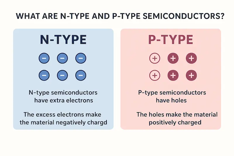
What Is an N-Type Semiconductor?
An N-type semiconductor is created when pure silicon is mixed with a small amount of another element that has more electrons, such as phosphorus or arsenic. These added atoms give the silicon extra electrons that can move freely inside the material, allowing an electric current to pass through more easily.
Because it has more negatively charged electrons, this material is called N-type, where the letter “N” stands for negative. N-type semiconductors are often used in modern solar technologies like TOPCon, HJT, and IBC solar cells. They are known for providing higher efficiency, performing better in warm conditions, and lasting longer than older designs.
What Is a P-Type Semiconductor?
A P-type semiconductor is made by adding a small amount of an element with fewer electrons than silicon, such as boron or gallium. This process creates tiny empty spaces in the silicon structure, called holes. These holes act as pathways that let electrons move through the material, carrying a positive charge.
Since these holes behave like positive carriers, the material is called P-type, where the letter “P” stands for positive. P-type semiconductors are widely used in traditional solar panels, including PERC and polycrystalline types. They are affordable, dependable, and a popular choice for home and commercial solar installations.
How N-Type and P-Type Semiconductors Work
Both N-type and P-type semiconductors play a key role in how solar cells generate electricity. They work together to create a constant movement of electric charges when sunlight hits the panel.
In an N-type semiconductor, there are extra electrons that move freely inside the material. These electrons are negative charge carriers. In a P-type semiconductor, there are fewer electrons, which means it has more empty spaces called holes. These holes act as positive charge carriers.
When the two materials are placed together inside a solar cell, they form a PN junction — a thin boundary where the N-type and P-type layers meet. At this junction, some electrons from the N-type side move across to fill the holes on the P-type side. This movement creates a small electric field that stops the charges from mixing completely.
When sunlight hits the solar cell, the energy from the light knocks electrons loose from their atoms. The built-in electric field at the PN junction pushes these free electrons toward the N-type side and the holes toward the P-type side. This movement of charges creates a steady flow of electricity through an external circuit.
In simple terms, the N-type layer provides the electrons, the P-type layer provides the holes, and together they make the solar cell generate clean, usable power from sunlight.
Key Differences Between N-Type and P-Type Semiconductors
N-type and P-type semiconductors both help solar panels turn sunlight into electricity, but they are not the same. The way they are made affects their performance, cost, and lifespan.
Ease of Use
When comparing how easy they are to use, both N-type and P-type semiconductors have their strengths.
N-Type Semiconductors:
- Often need more advanced manufacturing methods.
- Require precise control during production.
- Usually used in high-efficiency solar panels or modern devices.
P-Type Semiconductors:
- Easier to produce with simple techniques.
- Common in most standard solar panels.
- Readily available and well-understood by manufacturers.
Verdict:
If you prefer simplicity and easy handling, P-type semiconductors are better. But if you want advanced technology, N-type semiconductors have the edge.
Features
When looking at their key features, both types offer different advantages.
N-Type Semiconductors:
- Have extra electrons as charge carriers.
- Works well in low-light and high-temperature conditions.
- Show strong resistance against Light-Induced Degradation (LID).
P-Type Semiconductors:
- Use “holes” as charge carriers.
- Perform consistently under standard sunlight conditions.
- Offer reliable output for general applications.
Verdict:
N-type semiconductors offer more advanced features, while P-type semiconductors provide dependable, steady performance.
Performance
When comparing their performance, efficiency, and durability play a big role.
N-Type Semiconductors:
- Deliver higher conversion efficiency.
- Maintain performance longer over time.
- Handle temperature changes better.
P-Type Semiconductors:
- It has slightly lower efficiency.
- May show small performance drops with time due to LID.
- Still provides solid output for residential use.
Verdict:
If performance and longevity matter most, N-type semiconductors are the better choice.
Pricing
When it comes to cost, there is a clear difference between the two.
N-Type Semiconductors:
- Usually cost more due to advanced materials and production steps.
- Offer better long-term value through higher efficiency.
P-Type Semiconductors:
- More affordable and widely available.
- Suitable for users with limited budgets.
Verdict:
For a lower upfront cost, P-type semiconductors are ideal. But for a higher value over time, N-type semiconductors make more sense.
Support
When considering support and availability, accessibility can influence your choice.
N-Type Semiconductors:
- Gaining popularity in the solar industry.
- Supported by top brands like Jinko, JA Solar, and Longi.
- Still newer, so local support may vary in some regions.
P-Type Semiconductors:
- Well-established with a strong global supply.
- Easier to find installers and replacement parts.
- Backed by years of production experience.
Verdict:
If you want easy availability and local support, P-type semiconductors are the safer option. But if you prefer newer technology with growing industry backing, N-type semiconductors are worth considering.
Here is a key difference comparison table of n-type and p-type semiconductors.
| Feature | N-Type Semiconductor | P-Type Semiconductor |
|---|---|---|
| Doping Element | Made by adding elements that have more electrons, such as phosphorus or arsenic. | Made by adding elements that have fewer electrons, such as boron or gallium. |
| Type of Charge Carrier | Electrons (negative charge carriers). | Holes (positive charge carriers). |
| Efficiency | Usually offers higher efficiency because electrons move more easily. | Slightly lower efficiency compared to N-type cells. |
| Light-Induced Degradation (LID) | Resistant to LID, keeping stable performance for many years. | Can lose some efficiency after long exposure to sunlight. |
| Conductivity | Has higher electrical conductivity. | Has moderate electrical conductivity. |
| Cost and Lifespan | More expensive to produce but lasts longer. | Lower cost but shorter lifespan. |
| Common Applications | Used in advanced solar panels such as TOPCon, HJT, and IBC. | Used in traditional solar panels like PERC and Polycrystalline types. |
Summary:
N-type semiconductors provide higher performance, stronger resistance to sunlight degradation, and a longer lifespan. P-type semiconductors are more affordable and widely used in standard solar systems.
Pros and Cons of N-Type and P-Type Semiconductors
Both N-type and P-type semiconductors have their own strengths and weaknesses. Understanding these helps users choose the right type based on their needs, budget, and long-term goals. Below are the main pros and cons of each type, written in simple and clear language.
Advantages of N-Type Semiconductors
There are many advantages, like
- Delivers higher power output in the same sunlight conditions.
- Maintains performance better in high temperatures.
- Resists light-induced degradation (LID) and PID effects.
- Offers a longer lifespan and slower performance loss.
- Performs better in shaded or low-light areas.
- Suitable for large-scale and premium solar installations.
Cons of N-Type Semiconductors
Here is a list of the cons of N-type solar cells
- Higher manufacturing and purchase costs.
- Slightly complex production process.
- Limited availability compared to P-type panels.
- Repairs and replacements can cost more.
Pros P-Type Semiconductors
Here is a list of the main benefits of P-Type Semiconductors.
- More affordable and widely available in the market.
- Proven technology with years of field performance.
- Easier and cheaper to produce.
- Works well for small homes and commercial setups.
- Offers a good balance between price and performance.
Cons of P-Type Semiconductors
Here is a list of the drawbacks of P-Type Semiconductors
- Slightly lower efficiency compared to N-type.
- More is affected by light-induced degradation.
- Shorter lifespan under harsh sunlight conditions.
- Performance can drop faster over time.
Summary:
N-type semiconductors are the better choice for users who want higher efficiency, better durability, and long-term value. P-type semiconductors are ideal for those who prefer a budget-friendly option that still delivers reliable performance.
Which Type Is Better?
Both N-type and P-type semiconductors have their place in solar technology. The right choice depends on your budget, energy goals, and how long you plan to use your system.
Choose P-type panels if you are looking for a budget-friendly option that offers dependable, standard performance. They are a good fit for homes, small businesses, or anyone wanting a cost-effective solar setup without needing top-tier efficiency.
Choose N-type panels if you want maximum efficiency, strong performance over time, or have limited roof space and need to get the most power from fewer panels. They are also ideal for long-term users who value durability and stable output.
Today, the solar industry is gradually moving toward N-type technology because it provides better performance and longer life. While P-type panels remain the most common choice for now, N-type panels are becoming the future standard for high-quality solar systems.
FAQs about N-Type and P-Type Solar Cells
Here are frequently asked questions
The main difference lies in how they carry an electric charge. N-type semiconductors have extra electrons that move freely, while P-type semiconductors have tiny empty spaces called holes that allow electricity to flow. N-type cells use electrons as the main carriers, and P-type cells use holes.
N-type solar cells are more efficient because electrons move faster and face fewer obstacles inside the material. They also resist light-induced degradation (LID), which means they keep their performance longer, even after years of sunlight exposure
Yes, P-type panels are still a solid choice for homes. They are more affordable, easy to find, and provide reliable performance for most residential systems. While they are slightly less efficient than N-type panels, they offer great value for users who want a cost-effective solar solution.
Conclusion
N-type and P-type semiconductors both play an important role in modern solar technology. The main difference is how they move electric charge. N-type uses electrons, while P-type uses holes. N-type panels offer higher efficiency and longer life. P-type panels give reliable performance at a lower price. Each type has its own benefits depending on your needs. Now that you know the key differences between N-type and P-type semiconductors, choose the one that fits your energy goals best.


- Be Respectful
- Stay Relevant
- Stay Positive
- True Feedback
- Encourage Discussion
- Avoid Spamming
- No Fake News
- Don't Copy-Paste
- No Personal Attacks
- Be Respectful
- Stay Relevant
- Stay Positive
- True Feedback
- Encourage Discussion
- Avoid Spamming
- No Fake News
- Don't Copy-Paste
- No Personal Attacks
